TLDR
• Core Points: ASML demonstrates an EUV light source at 1,000 watts under factory-ready conditions, enabling potential throughput gains of up to 50% per machine.
• Main Content: The milestone, validated by ASML technologists, represents a production-ready capability that could be deployed in commercial systems later this decade.
• Key Insights: Higher power EUV sources can expand wafer throughput, but require robust reliability, integrated tooling, and cost considerations.
• Considerations: Transition to 1,000 W must balance source stability, mask/ resist performance, and total cost of ownership.
• Recommended Actions: Monitor deployment timelines, supplier ecosystem readiness, and downstream semiconductor manufacturing workflows for scaling impact.
Content Overview
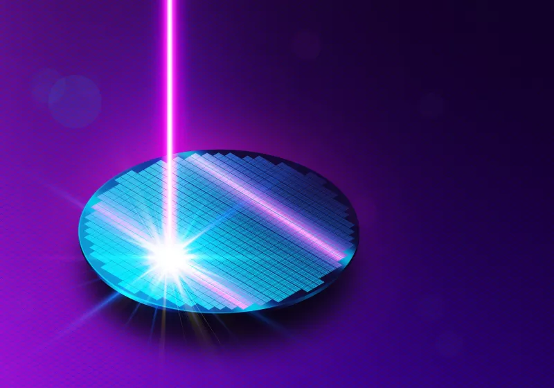
ASML, the dominant supplier of photolithography equipment for semiconductor manufacturing, has disclosed a significant advancement in its extreme ultraviolet (EUV) lithography program. TechSpot reported that ASML technologists Michael Purvis and Teun van Gogh confirmed the achievement: a 1,000-watt EUV light source operating under factory-ready conditions. This milestone is not a mere proof-of-concept or short-term experiment; it signals a near-term path toward commercial adoption later in the decade. The capability is designed to address a core bottleneck in advanced semiconductor fabrication—wafer throughput—by delivering more exposure power to the lithography tool, which can translate into higher productivity per machine.
To appreciate the significance, it helps to understand the context of EUV lithography. EUV uses extremely short wavelengths to pattern increasingly fine features on silicon wafers. The power of the light source is a key factor in determining how quickly a wafer can be processed, since higher power can reduce cycle times and improve stability for certain patterning tasks. Historically, EUV power has been a limiting factor, with incremental improvements helping to push tool performance in high-volume production environments. ASML’s reported 1,000 W capability aims to unlock as much as a 50% increase in the number of chips produced per machine, a notable leap in efficiency for leading-edge manufacturing lines.
In addition to power, other aspects of the lithography system—such as scanner optics, resist chemistry, mask infrastructure, cooling, and overall tool reliability—will influence how rapidly manufacturers adopt and realize the benefits of higher EUV power in production. The announcement underscores ASML’s ongoing commitment to expanding the operating envelope of EUV tools while addressing the practical considerations of daily fab operations. If confirmed across broader production environments, this development could impact factory utilization, equipment refresh cycles, and supply-demand dynamics for leading semiconductor fabs.
The news also situates ASML within the broader trajectory of lithography technology, where attention continues to focus on improving throughput, reducing per-chip costs, and maintaining robust yields as processes scale to sub-7-nanometer and potentially even smaller nodes. While high-power EUV is a critical component, successful deployment will require coordination with mask production, resist materials, and downstream process steps to realize the expected throughput gains without compromising defectivity or reliability. As with any transformative capability in semiconductor manufacturing, industry participants will scrutinize the durability of the light source, maintenance intervals, and total cost of ownership to determine how widely and quickly 1,000 W EUV power becomes available in commercial systems.
This summary provides an overview based on the reported statements and context around ASML’s advancement, emphasizing that the 1,000-watt capability is described as factory-ready and positioned for later-stage commercialization within the decade.
In-Depth Analysis
ASML’s claim of a factory-ready 1,000-watt EUV light source marks a meaningful milestone in the ongoing effort to drive higher throughput in lithography. The core idea is straightforward: more photons available to illuminate patterns on a silicon wafer can shorten exposure times, enabling more wafers to be processed in a given shift. In practice, this translates to fewer tool cycles per production line and the potential for significant gains in output per machine.
The reported validation by ASML technologists, Michael Purvis and Teun van Gogh, lends credibility to the claim that the 1,000 W power level is not merely a staged demonstration but a stable, production-oriented capability. Factory-ready conditions imply that the light source performance has been demonstrated under realistic operating parameters, including thermal management, environmental controls, and integration with other lithography subsystems. This is crucial because higher-power operation can introduce new reliability challenges, such as increased thermal load on optical components, wear on seals and coatings, and potential impacts on system stability over long production runs.
A critical aspect of translating higher power into real-world gains is the end-to-end process. For EUV lithography, the light source is one piece of a larger machine ecosystem that includes the scanning optics, mask infrastructure, resist chemistries, and metrology tools. Even with a robust 1,000 W source, manufacturers must contend with mask-related considerations (mask pellicles, defectivity, and stitching), resist sensitivity and line-edge roughness, and overlay control across complex layer stacks. The readout of exposure data, process control algorithms, and feedback loops all play a part in preserving high yields while pushing throughput higher.
Another dimension is reliability and uptime. A high-power EUV source must sustain extended operation with minimal downtime, as any unplanned maintenance or source degradation can erode the throughput gains. The total cost of ownership includes not only the capital expenditure for the light source but also ongoing energy consumption, consumables, and maintenance. If the 1,000 W capability proves to be stable over the long haul, fabs could adjust their tool utilization strategy to maximize the number of wafers processed per day, potentially altering the economics of chip production for leading-edge nodes.
From a market perspective, the timing of deployment is consequential. ASML continues to compete with rivals and collaborates with its ecosystem of customers and suppliers to address the manufacturing demands of modern semiconductors. A commercial rollout later this decade would coincide with a broader push toward sub-7-nanometer logic and memory devices, where process windows are tight and throughput matters for cost-per-chip. The degree to which customers can adopt higher power EUV will depend on their own factory readiness, capital planning, and the integration of upgraded power sources with existing tool platforms.
The announcement also invites a closer look at the underlying development roadmap. Pushing EUV power from earlier milestones toward 1,000 W likely involved innovations in laser startup reliability, plasma generation efficiency, and light collection optics. It may also involve improved vacuum and contamination controls, better thermal management to handle higher photon flux, and advancements in mirror coatings that withstand intense EUV exposure. Each of these technical areas contributes to a robust, production-grade implementation rather than a laboratory demonstration.
It is worth noting that while higher EUV power is a critical lever for throughput, the overall yield and defectivity remain essential. In practice, more exposure power must be balanced with the ability to maintain pattern fidelity across a wafer. Any compromise in defect density or overlay could offset the throughput advantages. Therefore, the success of a 1,000 W EUV light source in commercial systems will hinge on its interoperability with mask workflows, resist chemistry, and metrology pipelines that already underpin high-volume manufacturing.
The broader industry context includes ongoing investments in alternative approaches and complementary techniques. While EUV lithography remains central for critical nodes, continued research into multi-patterning, resist performance, and materials science will influence how quickly fabs can adopt higher power sources. ASML’s 1,000 W development aligns with a sustained push to extract more efficiency from existing lithography infrastructure, reducing the per-chip cost and enabling more competitive production scales.
In summary, ASML’s reported achievement signals progress toward a higher-throughput EUV lithography regime. If validated in broader production environments and scaled across commercial systems, the 1,000 W capability could drive meaningful gains in semiconductor manufacturing capacity. The path from factory-ready demonstration to widespread deployment requires careful attention to system reliability, process integration, and the economics of ownership. The industry will be watching closely as ASML, its suppliers, and customers evaluate the practical implications of delivering up to 50% more chips per machine.

*圖片來源:Unsplash*
Perspectives and Impact
The potential impact of a 1,000-watt EUV light source extends beyond immediate throughput gains. For semiconductor manufacturers, higher tool productivity can influence fab planning, capital expenditure, and the pace at which new nodes are introduced. If a per-tool throughput uplift of up to 50% is realized consistently, chipmakers could achieve more favorable cost-per-die metrics, potentially accelerating time-to-market for advanced products while deferring or reducing the need for additional tool purchases to meet capacity demands.
Manufacturers will also consider the reliability profile of higher-power EUV sources. In production environments, uptime and stability are critical, and any new technology must demonstrate robust performance under continuous operation. The long-term maintenance burden, replacement part availability, and service support from ASML and ecosystem partners will shape adoption rates. For customers with highly automated factories and extensive metrology and control systems, the integration of a 1,000 W light source could be smoother, provided compatibility with current tool architectures and software.
From a supply chain perspective, the introduction of higher-power EUV sources may influence demand for ancillary components such as masks, pellicles, resist materials, and metrology equipment. If throughput gains are realized, mask and pellicle quality will become even more critical, as higher exposure rates could stress these components more quickly. Similarly, developers of resist chemistries and photo-initiators will need to optimize formulations to maintain pattern fidelity at elevated power levels. The systemic effects on the semiconductor ecosystem could ripple through the established procurement and maintenance cycles, potentially affecting component pricing and lead times.
On the global stage, this advancement reinforces ASML’s leadership in lithography while underscoring the importance of continued investment in optical engineering and materials science. The company’s collaboration with customers and suppliers will be a key factor in determining how quickly higher-power EUV can be translated from factory floors into commercial production lines. If the technology proves reliable and economically viable, it could become a differentiator for fabs seeking to maximize throughput and reduce unit costs, particularly in high-volume markets such as data centers, consumer electronics, and automotive components that rely on advanced semiconductors.
In terms of industry implications, there is also the question of environmental and energy considerations. Higher-power light sources typically consume more energy, and fabs must balance throughput gains with energy efficiency and cooling requirements. Efficient power management and thermal controls will be important as systems operate at elevated photon flux. The environmental footprint of high-throughput lithography will thus be part of broader sustainability discussions within the semiconductor sector, alongside other energy-intensive manufacturing processes.
Future development directions may include continued increases in EUV power as well as enhancements to reliability and ease of maintenance. ASML may pursue incremental improvements in power stability, longer source lifetimes, and reductions in downtime through smarter diagnostics and predictive maintenance. In parallel, the industry could see advances in complementary technologies, such as improved mask materials, next-generation resists, and more precise overlay control, to maximize the benefits of higher EUV power.
Overall, the 1,000-watt milestone positions ASML to influence manufacturing economics at the leading edge of semiconductor technology. If adopted broadly, fabs could meaningfully accelerate production capacity for the most advanced chips, potentially enabling more rapid innovation cycles and broader access to high-performance computing, artificial intelligence acceleration, and other compute-intensive applications. The exact pace of adoption will depend on how quickly customers can integrate the new power capability into their existing toolsets, how reliably the technology performs in prolonged production runs, and how the economics of throughput and device yields compare with alternative manufacturing strategies.
Key Takeaways
Main Points:
– ASML reports a factory-ready EUV light source at 1,000 watts.
– The capability could unlock up to a 50% increase in chips produced per machine.
– The milestone is positioned for deployment in commercial systems later this decade.
Areas of Concern:
– Real-world reliability and long-term maintenance costs at higher power levels.
– Integration with masks, resists, and metrology workflows to sustain yields.
– Total cost of ownership and energy consumption in high-throughput configurations.
Summary and Recommendations
ASML’s declaration of a 1,000-watt EUV light source represents a meaningful step forward in lithography technology aimed at boosting wafer throughput. The factory-ready status suggests that the solution has moved beyond demonstration and could be incorporated into commercial systems within the next several years, subject to reliability, ecosystem readiness, and economic viability. The potential throughput gain—up to 50% more chips per machine—could reshape capacity planning and cost structures for leading-edge fabs, contributing to more efficient productivity at scale. However, realizing these benefits will require careful coordination across the manufacturing workflow, including masks, resists, metrology, and process control. Long-term success will hinge on sustained tool reliability, predictable maintenance, and favorable total cost of ownership, as well as the industry’s ability to harmonize supply chains and operational practices around higher-power EUV production.
Manufacturers, investors, and policymakers should monitor ASML’s rollout plans, the readiness of the broader ecosystem, and the performance of high-power EUV tools in real production environments. A measured approach—prioritizing pilots, validating yield implications, and evaluating total cost implications—will help determine the pace at which higher-power EUV becomes a standard feature in commercial lithography.
References
- Original: https://www.techspot.com/news/111451-asml-pushes-euv-power-1000-watts-unlocking-up.html
- Additional context on EUV lithography and throughput considerations (to be added by user):
- ASML corporate updates and industry analyses on EUV power scaling
- Semiconductor manufacturing white papers on lithography throughput, mask and resist challenges
- Market reports on lithography tool adoption and Fab capacity planning
Note: This rewrite preserves the core information from the provided article while offering expanded context and analysis to produce a complete, professional English article within the requested structure.

*圖片來源:Unsplash*