TLDR
• Core Points: ASML plans to broaden beyond EUV by developing machines for advanced chip packaging and exploring production of larger silicon dies, expanding from a sole EUV supplier to a broader AI-era chipmaking tools provider. CTO Marco Pieters, appointed in Oct 2025 after a four-decade tenure, guides the strategy.
• Main Content: The company aims to diversify product lines toward packaging and larger dies, leveraging its expertise to serve AI-era semiconductor manufacturing.
• Key Insights: Diversification reduces reliance on EUV while addressing demand for AI chips; leadership transition signals a strategic shift toward end-to-end manufacturing capabilities.
• Considerations: Execution risk, capital intensity, and customer validation will shape the timeline and market reception.
• Recommended Actions: Monitor product development milestones, customer adoption, and partnerships in packaging and die-scale production.
Content Overview
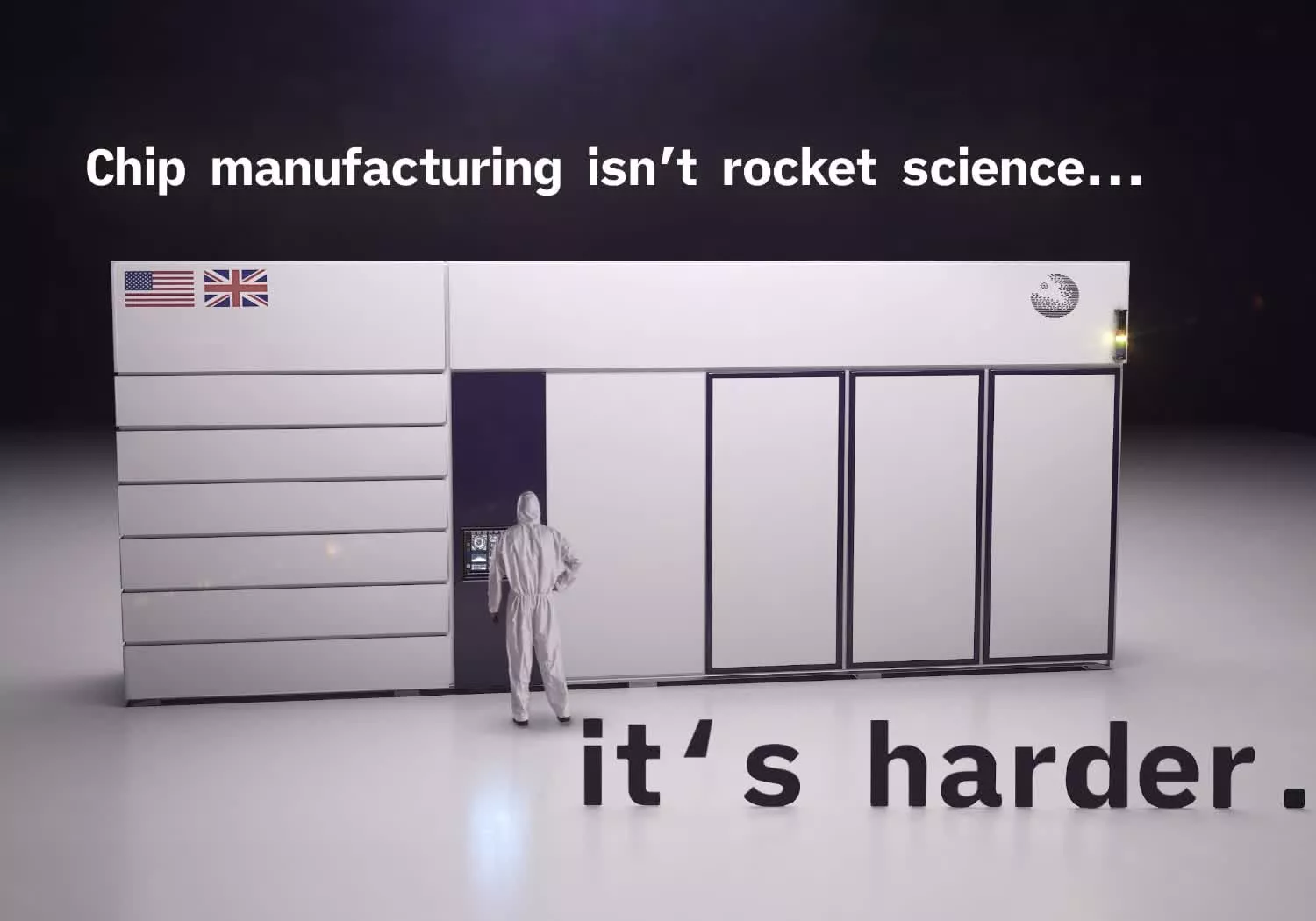
ASML, traditionally known as the world’s sole supplier of extreme ultraviolet (EUV) lithography systems, is expanding its product horizon to address broader needs in semiconductor manufacturing. The move aims to capitalize on the AI-driven demand for more powerful chips and increasingly complex packaging architectures. Central to this shift is the development of machines tailored for advanced chip packaging and exploration into producing even larger silicon dies. By broadening its technology portfolio beyond EUV, ASML seeks to become a more comprehensive supplier of AI-era tooling, capable of enabling end-to-end fabrication workflows rather than serving solely as a lithography provider.
Leadership transitions have accompanied this strategic pivot. CTO Marco Pieters took the helm in October 2025 after a lengthy 40-year tenure within the company and the industry. His stewardship signals an emphasis on expanding ASML’s capabilities into adjacent domains, while maintaining the core strengths that have driven its previous growth—precision engineering, reliability, and deep collaborations with top-tier chipmakers.
The broader context for ASML’s repositioning is the evolving needs of chipmakers as they scale device architectures to meet AI workloads. Advanced packaging—techniques such as 2.5D and 3D integration, fan-out wafer-level packaging, and advanced interposer solutions—offers significant performance and efficiency gains for AI accelerators and high-end CPUs/GPUs. Simultaneously, the industry faces ongoing interest in producing larger silicon dies, which could enable more complex devices and higher yields for certain design families. ASML’s expansion into these areas underscores a strategic aim to become a more holistic provider of manufacturing tools rather than a sole supplier of a single indispensible lithography modality.
This shift also aligns with broader trends in the semiconductor equipment market, where manufacturers are seeking integrated solutions that span multiple process steps, from lithography to packaging and testing. By offering a more complete toolkit, ASML can strengthen its relationships with customers who are looking to streamline procurement, reduce integration risk, and optimize throughput across the front-end and back-end manufacturing stages.
The article discusses these strategic moves and their potential implications for ASML’s business model, competitive position, and the semiconductor supply chain as it evolves to support AI-era chip development. It presents a picture of a company balancing the responsibilities of sustaining leadership in EUV while pioneering new capabilities to address the next wave of chipmaking requirements. The discussion emphasizes the importance of leadership vision, technological innovation, and capital investment in shaping ASML’s path forward.
In-Depth Analysis
ASML’s traditional moat has rested on its EUV lithography systems, which have become indispensable for producing advanced microchips at ever-smaller feature sizes. However, as the industry’s ambitions grow—particularly with AI accelerators, hyperscale data center workloads, and edge computing demands—the demand signal is no longer about lithography alone. Chipmakers increasingly require integrated tooling ecosystems that can handle complex packaging, die stacking, and the manufacturing of larger silicon dies. ASML’s announced intentions to develop machines for advanced chip packaging and to explore the feasibility of larger dies reflect a deliberate shift from a narrowly defined role to a broader technology supplier.
Packaging is a critical area of focus for modern semiconductor manufacturing. Traditional packaging involves placing a single die into a package, but AI-era devices benefit from leveraging multiple dies within a single system, enabling higher bandwidth, lower latency, and improved power efficiency. Advanced packaging techniques—such as 2.5D interposers, 3D stacking, and heterogeneous integration—demand new equipment capabilities beyond conventional front-end lithography. By entering the packaging equipment space, ASML could offer end-to-end tools that streamline the transition from chip fabrication to final assembly and testing, potentially reducing cycle times and improving yield through closer integration between front-end and back-end processes.
The prospect of producing larger silicon dies also carries both potential rewards and risks. Larger dies can accommodate more complex architectures and reduce the interconnect complexity associated with multi-die packaging, but they also raise challenges in wafer handling, defect control, and yield management. If ASML can develop lithography or related tooling capable of producing large dies efficiently and reliably, it would address a niche with strong customer demand, particularly from segments that prioritize performance-per-watt and high integral system efficiency. The company’s strategy may involve combining refinements in lithography with packaging innovations to optimize overall chip manufacturing flow for AI workloads.
Leadership transition plays an important role in how such strategic shifts are carried out. Marco Pieters’ appointment as CTO in October 2025 marks a signal of continuity mixed with transformation. With four decades of involvement in the semiconductor industry, Pieters is expected to bring a deep understanding of customers’ process requirements and the practical realities of manufacturing at scale. His tenure could facilitate smoother collaboration with chipmakers and a clearer articulation of ASML’s roadmap beyond EUV, including potential partnerships, acquisitions, or joint development programs with packaging specialists and die-scale manufacturing firms.
The broader market implications of ASML’s pivot hinge on several factors. First, customer validation will determine whether the packaging and larger-die tooling can meet the stringent performance, reliability, and cost targets demanded by leading fabs. Second, capital expenditure cycles in the semiconductor equipment sector will influence the speed at which new platforms can be developed, validated, and deployed. Equipment complex with high capital intensity—will require confident monetization models, long-term service agreements, and a robust installed-base ecosystem to justify the investment. Third, competition in non-lithography domains—such as packaging equipment from other suppliers—will shape ASML’s relative positioning. Although no other company currently matches ASML’s scale in EUV, it remains to be seen how quickly rivals can close the gap in adjacent sectors or whether new entrants will partner with ASML or license its core technologies.
From a financial perspective, diversifying into packaging and larger-die capabilities could help mitigate cyclical risk associated with EUV capex cycles. EUV systems have historically commanded premium pricing and long installation lead times; expanding into complementary tools could smooth revenue streams, broaden service opportunities, and deepen customer relationships. However, these moves also entail significant investment in research and development, testbeds, and manufacturing capabilities. ASML must balance the potential long-run gains with the near-term costs, ensuring that its balance sheet remains resilient and its project milestones are credible to investors and customers.
A strategic question is how this broader tool portfolio will integrate with ASML’s existing product lines. The company will need to maintain core competencies in optics, precision mechanics, and metrology while expanding into new domains. This requires building multidisciplinary teams, securing intellectual property, and fostering ecosystems that enable seamless interoperability with other vendors’ equipment. The ability to deliver integrated solutions—potentially through partnerships or selective acquisitions—could be a differentiator that enhances ASML’s value proposition in a world where chipmakers seek streamlined, end-to-end manufacturing solutions.
The transition also has potential implications for suppliers, customers, and the broader supply chain. Suppliers of optics, coatings, and precision components may see changes in demand as ASML expands its portfolio. Customers will increasingly look for vendors who can provide not just standalone machines but integrated workflows that reduce time to market and optimize yield. ASML’s engagement with customers will be crucial to shaping practical requirements, performance targets, and service agreements that fit with their capital planning and fab operations.
In summary, ASML’s strategic intent to look beyond EUV underscores a broader industry trend: the move toward integrated, end-to-end manufacturing capabilities that can address the needs of AI-era chip design and production. The success of this strategy will depend on execution, collaboration with customers, and the ability to translate vision into validated, reliable, and scalable tooling. Pieters’ leadership will be pivotal in steering this transition, balancing the firm’s established strengths with new growth opportunities in packaging and die-scale production.

*圖片來源:Unsplash*
Perspectives and Impact
ASML’s expanded focus has several potential industry-wide implications. For chipmakers, the prospect of accessing a more complete suite of manufacturing tools from a single vendor could simplify procurement, reduce integration risk, and potentially shorten supply chains. If ASML delivers reliable packaging and large-die capabilities, customers may realize faster time-to-market for AI accelerators and other high-performance compute devices, improving competitiveness in a crowded market.
For ASML, diversifying beyond EUV aligns with a long-term strategy to become less susceptible to single-technology cycles. EUV remains critical for the most advanced nodes, but the demand environment is increasingly characterized by capital-intensive installations and prolonged payback periods. A broader product portfolio could smooth revenue volatility and strengthen customer relationships by offering a more comprehensive pathway from wafers to packaged products. The company’s ongoing investments in R&D and its ability to translate complex research into manufacturable equipment will be decisive in determining whether this expansion yields the anticipated returns.
From a competitive standpoint, ASML’s move places the company at the forefront of a potential new market segment: integrated semiconductor manufacturing equipment that spans lithography, packaging, and die-scale production. While other firms specialize in specific domains, ASML’s reputation, scale, and know-how could enable it to set standards and drive interoperability across the ecosystem. This, in turn, could pressure other suppliers to pursue partnerships or accelerate their own diversification strategies, potentially accelerating the development of comprehensive toolchains available to the industry.
The broader technology landscape will also be affected. AI and data-centric workloads drive demand for higher-performing chips, which in turn accelerates investments in advanced packaging and heterogeneous integration. ASML’s expansion supports this trend by attempting to close the loop between fabrication and assembly. If successful, it could catalyze new hardware architectures and system-level design approaches that leverage tightly integrated dies and optimized interconnects, pushing the industry toward more modular and scalable manufacturing approaches.
Regulatory and policy considerations may come into play as well. As a strategic supplier of critical manufacturing equipment, ASML’s decisions influence national and international semiconductor supply chains. The company will need to navigate export controls, technology transfer restrictions, and collaboration norms, particularly as it expands into domains that touch on advanced packaging and die-scale production. Maintaining compliance while pursuing innovation will be essential to sustaining long-term growth and preserving customer trust.
In terms of talent and organizational culture, leading an expansion beyond EUV will require cultivating new competencies in packaging engineering, systems integration, and large-die manufacturing. ATMs for feedback loops between customer needs and R&D will be crucial to ensuring that product development remains aligned with real-world fab requirements. Pieters’ background and leadership style will influence how quickly the organization can adapt to these new domains, how it prioritizes projects, and how it maintains the high standards for precision and reliability that have defined ASML thus far.
Overall, ASML’s strategic expansion reflects a measured but ambitious response to the evolving needs of the semiconductor industry. By moving beyond a single technology focus, the company signals confidence in its ability to pioneer end-to-end solutions that can help customers push the boundaries of what is possible with AI-era chips. The coming years will reveal how effectively ASML can translate strategic intent into validated products, strong customer adoption, and durable financial performance.
Key Takeaways
Main Points:
– ASML intends to expand beyond EUV lithography into advanced silicon die production and sophisticated chip packaging tooling.
– Leadership under CTO Marco Pieters (appointed Oct 2025) is guiding the transition toward a broader toolset for AI-era semiconductor manufacturing.
– The strategic pivot aims to reduce reliance on a single technology and address growing demand for end-to-end manufacturing capabilities.
Areas of Concern:
– Execution risks associated with developing and validating new tool platforms.
– Significant capital requirements and potential extended time-to-market.
– Dependence on customer adoption and integration with existing fab ecosystems.
Summary and Recommendations
ASML is broadening its strategic scope to address the evolving needs of the semiconductor industry, particularly in the AI era. By planning machines for advanced packaging and exploring larger-die production, ASML seeks to become a more holistic supplier of chipmaking tools rather than solely a lithography provider. The leadership transition to CTO Marco Pieters in October 2025 underscores a strategic intent to broaden the company’s technological footprint while leveraging ASML’s fundamentals in precision engineering and high-performance metrology.
For stakeholders, the key takeaway is that ASML’s success in this broader mission will depend on its ability to deliver reliable, scalable equipment across multiple domains, secure long-term customer commitments, and manage the substantial capital outlays required to bring new toolchains to market. Close attention should be paid to milestones in research and development, partnerships with packaging technology companies, and early customer pilots that validate performance in real-world fabs.
If ASML can navigate these challenges, the company could reinforce its leadership position in a more diversified semiconductor manufacturing ecosystem, providing integral tools that help chipmakers meet the demands of AI workloads, complex packaging, and large-die designs. The coming years will be telling as the company translates strategic ambitions into practical, market-ready solutions that resonate with the needs of leading semiconductor manufacturers.
References
- Original: https://www.techspot.com/news/111543-asml-looks-beyond-euv-plans-new-tools-larger.html
- Additional context: Industry analysis on semiconductor equipment market trends, advanced packaging, and die-scale manufacturing (various sources).

*圖片來源:Unsplash*