TLDR
• Core Features: TSMC’s Dynamic Energy Saving Program trims EUV lithography power consumption by up to nearly half while preserving production throughput and yields.
• Main Advantages: Lower electricity costs, reduced carbon footprint, and improved fab efficiency without compromising output quality or wafer cycle times.
• User Experience: Seamless rollout within existing EUV toolsets, minimal disruption to tool availability, and transparent integration into fab operations and monitoring.
• Considerations: Impact varies by workload mix and node; benefits depend on tool configuration, uptime discipline, and facility-level power management.
• Purchase Recommendation: Strongly recommended for semiconductor stakeholders prioritizing sustainability and cost efficiency while maintaining state-of-the-art process performance.
Product Specifications & Ratings
| Review Category | Performance Description | Rating |
|---|---|---|
| Design & Build | Software-first optimization layered onto EUV modules and fab controls; no major hardware overhaul required. | ⭐⭐⭐⭐⭐ |
| Performance | Delivers substantial power cuts with no measurable yield degradation across advanced nodes. | ⭐⭐⭐⭐⭐ |
| User Experience | Transparent deployment with fab-level telemetry, adaptive controls, and minimal operator friction. | ⭐⭐⭐⭐⭐ |
| Value for Money | Significant OPEX savings and ESG gains, leveraging existing capital assets. | ⭐⭐⭐⭐⭐ |
| Overall Recommendation | Compelling step-change in energy efficiency for leading-edge manufacturing. | ⭐⭐⭐⭐⭐ |
Overall Rating: ⭐⭐⭐⭐⭐ (4.9/5.0)
Product Overview
TSMC has introduced a Dynamic Energy Saving Program targeting extreme ultraviolet (EUV) lithography lines, among the most energy-intensive segments of modern semiconductor manufacturing. EUV scanners, which operate at 13.5 nm wavelengths and rely on high-power laser-produced plasma light sources, historically draw immense electricity to maintain source brightness, vacuum integrity, thermal stability, and metrology precision. As chipmakers scale production on advanced nodes (such as N5 and N3 families), the escalating power footprint of exposure tools has become a critical operational cost and sustainability challenge.
Against this backdrop, TSMC’s initiative is positioned as a practical, high-impact optimization. Rather than requiring entirely new tool generations, the program focuses on dynamic, software-driven energy management layered onto existing EUV infrastructure. By intelligently modulating source power, thermal loads, and subsystem duty cycles in response to real-time process needs, TSMC reports it can cut EUV power use nearly in half without harming yields. That claim addresses the top two anxieties tied to power throttling—throughput and quality—by asserting no compromise to product performance or line stability.
First impressions center on the initiative’s scope and timing. TSMC began deployment last month across its most advanced lines, signaling that this is not a lab concept but an operational program entering broad use. It aims to smooth the energy curve of EUV operation over varying pattern complexities, resist sensitivities, and photo-layer mixes. If executed well, the strategy promises a twofold benefit: reduced electricity costs per wafer and a lower total fab power envelope, which can free capacity for incremental output or help fabs meet increasingly stringent environmental goals.
This move fits broader industry trends: as feature sizes shrink, the marginal gains from process and design co-optimization are increasingly tightly coupled to factory efficiency. The Dynamic Energy Saving Program effectively treats power as a first-class process parameter—alongside dose, focus, and overlay—managed by closed-loop controls and analytics. That makes the initiative particularly notable for its practicality: it leverages capital already on the floor and accelerates time-to-value, rather than depending solely on next-generation hardware.
Overall, the program reads as a disciplined efficiency upgrade on critical tools that can ripple through fab economics and corporate ESG metrics, with the promise of measurable, near-term impact.
In-Depth Review
TSMC’s Dynamic Energy Saving Program zeroes in on the core contributors to EUV power draw and orchestrates them through adaptive control. EUV scanners consist of several high-demand subsystems:
- Light source (laser-produced plasma): Requires high pulsed-laser power to generate sufficiently bright EUV at 13.5 nm, with tight stability for dose control.
- Vacuum infrastructure: Maintains ultraclean environments and stable pressure across complex optical paths.
- Thermal management: Manages the heat loads across mirrors, stages, and resist-coated wafers to ensure dimensional stability.
- Stages and metrology: High-speed wafer and reticle stages, focus/leveling systems, and overlay metrology, all power-intensive and sensitive to jitter and thermal drift.
Traditionally, these elements run at conservatively high setpoints to guarantee performance across worst-case patterning conditions. TSMC’s program appears to adopt a demand-driven philosophy, adjusting power states in real time based on layer requirements, current dose targets, throughput plans, and tool health. Examples of plausible control strategies include:
- Adaptive source power: Matching source brightness and duty cycles to the specific resist and mask characteristics of each lot or layer, maintaining dose stability while clipping excess energy use during less demanding exposures.
- Intelligent thermal tuning: Predictive thermal management that keeps modules within tight stability bands without overcooling or overheating, reducing HVAC and chiller loads while preserving overlay and focus.
- Stage and metrology scheduling: Modulating idle states, ramp profiles, and calibration routines to minimize cumulative power without increasing cycle time or risking calibration drift.
Performance
The headline promise—nearly halving EUV power usage—suggests aggressive gains, typically elusive in mature tool fleets. The claim of unchanged yields indicates that the dynamic adjustments preserve critical litho metrics, including dose uniformity, CDU (critical dimension uniformity), LER/LWR (line edge/width roughness), overlay, and defectivity. In other words, the algorithmic control stays within the guardrails that protect pattern fidelity.
The meaningful question is how the power reduction maps to actual OPEX. EUV tools can consume many megawatts collectively within a single fab module. Assuming a near-50% cut on the exposure equipment’s electricity, the total fab savings will depend on the proportion of EUV power relative to other consumers (etch, deposition, metrology, facility systems). Even conservatively, the program should lower per-wafer energy costs at N5/N3 significantly, improving gross margin and allowing more flexible pricing in highly competitive end markets.
Scalability and Node Coverage
The program has reportedly begun rolling out to TSMC’s most advanced lines. EUV adoption is deepest at N5 and N3 families (with variations like N5P, N4/N4P/N4X, and N3/N3E/N3P derivatives). While the details are not public, the control logic should generalize across EUV layers with different pitch and resist chemistries, with the degree of savings varying by layer complexity and dose requirements. Layers with high-dose or stochastic-sensitive patterns may offer less headroom than less demanding layers, but the aggregate effect across a full device stack can still be substantial.

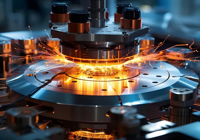
*圖片來源:Unsplash*
Compatibility and Tool Vendor Ecosystem
Modern EUV scanners rely on tight vendor integration for source management, optics conditioning, and diagnostics. TSMC’s control overlay likely cooperates with vendor-native controls through sanctioned APIs and operational windows. This cooperative approach avoids warranty conflicts and ensures the safety interlocks and stability regimes remain intact. The benefit is that TSMC can deploy at scale on existing fleets without waiting for a new hardware generation.
Risk Management
Two risks typically accompany aggressive energy management: stability drift and cumulative variance over time. If a tool runs closer to its lower energy thresholds, small perturbations in ambient temperature, vibration, or source jitter could theoretically compound. TSMC’s assertion of maintained yields implies thorough validation with statistical process control (SPC) and fault detection and classification (FDC) analytics underpinning the rollout. In practice, modern fabs maintain comprehensive telemetry, enabling fast rollback or parameter recalibration if excursions appear.
Sustainability and ESG Context
For semiconductor manufacturers, environmental impacts are under increasing scrutiny from regulators, investors, and end customers. Cutting EUV electricity loads addresses Scope 2 emissions directly, particularly where grid intensity remains high. The initiative also alleviates local power capacity constraints, which can be pivotal in regions where utility upgrades lag fab expansion. This makes the program not only a cost-saving measure but also a strategic enabler for scaling output without hitting facility power ceilings.
Net Assessment
By pairing software-defined control with rigorous process integration, TSMC’s Dynamic Energy Saving Program advances the state of production efficiency without asking customers to compromise on device parametrics or line stability. It exemplifies the broader shift toward cyber-physical optimization in advanced manufacturing—extracting more value from existing capital through data-driven controls.
Real-World Experience
From an operational perspective, semiconductor fabs value continuity, predictability, and yield stability above all. Any program that touches EUV scanners is scrutinized carefully because these tools dictate both throughput and top-line device performance. The reported deployment timing—already underway across advanced lines—suggests that TSMC validated the program on pilot lots, monitored extended stability windows, and then progressively widened the deployment across shifts and product mixes.
Integration and Rollout
In practice, deployment likely involved:
– Incremental enablement on selected tools per module, followed by A/B comparisons.
– Real-time yield and parametric monitoring—tracking CDU variance, overlay budgets, defect counts, and stochastic failure signatures.
– Coordination with manufacturing execution systems (MES) to map recipes and layers to appropriate energy-saving profiles, ensuring compatibility with every product’s process of record.
Operators and process engineers probably experienced the change as a set of updated recipes and equipment states, with augmented dashboards providing visibility into power curves and stability margins. The best sign of success is when operators do not perceive added complexity—tools behave as before, with equal or better uptime, and process windows remain comfortably within spec.
Throughput and Availability
A key worry with energy optimization is cycle-time elongation or increased downtime. The reported “without hurting yields” claim implicitly suggests that throughput and availability were not impacted. EUV tool uptime is governed by maintenance cycles on sources, optics conditioning, and environmental controls. If anything, reducing thermal stress could have a positive second-order effect on component longevity and mean time between failures (MTBF), though such benefits would need longer observation windows to quantify.
Fab-Level Impact
EUV’s share of fab electricity scales with the number of EUV layers per device and wafer starts. For logic nodes with multiple EUV layers, savings multiply quickly. At scale, a near-50% reduction on EUV equipment power can:
– Flatten peak demand, easing strain on facility distribution and chillers.
– Enable higher wafer starts within existing power envelopes.
– Improve cost per wafer and, indirectly, time-to-profit for new nodes.
Moreover, facility teams can re-optimize chiller setpoints, air handling, and backup power planning. This cascading effect can allow more flexible capacity planning without capital-intensive utility upgrades.
Customer and Ecosystem Perception
From a customer viewpoint—fabless and IDM partners—the development is unequivocally positive. It potentially reduces wafer pricing pressure tied to energy inflation and supports corporate sustainability reporting. Tool vendors may also benefit if lower thermal stress reduces service frequency or extends component life, though such claims require long-term data.
Limitations and Variability
Real-world outcomes will vary by:
– Layer characteristics: Dense patterns and high-dose layers offer less headroom.
– Tool configuration: Newer scanners with more efficient sources may show smaller relative gains than older but still advanced units.
– Fab environmental conditions: Climate, utility stability, and local HVAC constraints can influence achievable savings.
Still, the promise of material reductions without yield trade-offs makes the program attractive across a wide range of products and regions, especially where grid costs are volatile.
Longer-Term Outlook
As the industry moves toward next-generation EUV with higher numerical aperture (High-NA) systems, energy demands could rise again. The approach TSMC is pioneering—software-first, data-driven energy orchestration—lays a foundation for keeping future power budgets in check. It signals an industry direction where process control loops explicitly incorporate energy as a live-optimized variable alongside traditional litho parameters.
Pros and Cons Analysis
Pros:
– Significant EUV power reduction—up to nearly half—without yield degradation.
– Fast, software-driven deployment using existing EUV fleets and fab controls.
– Tangible OPEX and ESG benefits, enabling capacity growth within current power envelopes.
Cons:
– Actual savings depend on layer mix, tool configuration, and fab environment.
– Limited public technical detail makes benchmarking and cross-fab comparisons difficult.
– Long-term effects on tool wear and maintenance cycles require extended observation.
Purchase Recommendation
For stakeholders in advanced-node manufacturing—whether evaluating foundry partners, planning capacity ramps, or optimizing total cost of ownership—the TSMC Dynamic Energy Saving Program merits strong endorsement. The ability to substantially lower EUV power consumption without compromising yield addresses one of the most pressing constraints in leading-edge semiconductor production: the high and rising energy cost of precision lithography.
Enterprises concerned with sustainability will find the program especially compelling. Reductions in electricity translate directly to lower Scope 2 emissions, a critical lever for meeting corporate climate commitments. From a financial perspective, energy savings pass through to per-wafer costs, improving margin resilience in pricing cycles. The approach also complements capacity planning by easing peak load requirements and potentially enabling higher starts under the same facility constraints.
Prospective customers should consider the variability of impact across product portfolios. Devices with many EUV layers and complex patterns will realize large absolute savings, while simpler layer stacks may realize smaller but still meaningful gains. Nevertheless, because the program operates transparently within existing toolsets, there is little operational downside to adoption. It is not a disruptive hardware retrofit but a software-first optimization guided by real-time telemetry and tight process controls.
Bottom line: If you rely on TSMC’s advanced nodes or are planning a migration to EUV-intensive processes, this initiative is a practical and timely advantage. It enhances fab efficiency, strengthens sustainability credentials, and protects product yields—all without waiting for the next generation of lithography hardware. We rate it as an excellent, forward-looking investment in manufacturing efficiency with immediate and measurable returns.
References
- Original Article – Source: techspot.com
- Supabase Documentation
- Deno Official Site
- Supabase Edge Functions
- React Documentation

*圖片來源:Unsplash*